How to shrink giant resistors to fit in a small neural chip with quantum tunnelling
An ASIC (Application-Specific Integrated Circuit) is a chip designed to do one specific job, rather than a general-purpose chip like a CPU that can run any software. In a neural ASIC, that job is to read and process the tiny electrical signals from neurons.
Neural signals are very small and ride on top of slow electrical drift from the electrodes, so the amplifier needs a filter to block the drift while keeping the signal, and that requires enormous resistances (billions to trillions of ohms). A resistor that large would normally take up far more space than the entire chip, yet thousands of these channels must fit on a die a few millimeters across.
One way to solve this, and the one this essay builds up to, is to use the quantum wave function to make a resistor.
Explained below.
Fundamental
The following framework is useful in understanding the physical universe.
- Fundamental particles. Everything is built from a small set of particles, which fall into two families: fermions (matter, like electrons and quarks) and bosons (force-carriers, like the photon).
- Atoms. Quarks bind into protons and neutrons, which form a nucleus, which electrons surround.
- Molecules. Atoms bond together into structured groups.
- Statistical mechanics. When you have trillions of these particles, you stop tracking them individually and describe their collective behavior with probability.
- Thermodynamics. Out of that collective behavior emerge the everyday quantities we can measure such as temperature, pressure, energy.
- Bulk matter. Finally, solids, liquids, and gases can be explained.
The job of an ASIC is to control electricity, and inside the chip electricity is fundamental particles (electrons) moving around. In the brain the moving charges are ions, and the electrode is where one becomes the other. So to build a chip, we arrange atoms to steer individual electrons, in order to produce a useful behavior.
The silicon lattice
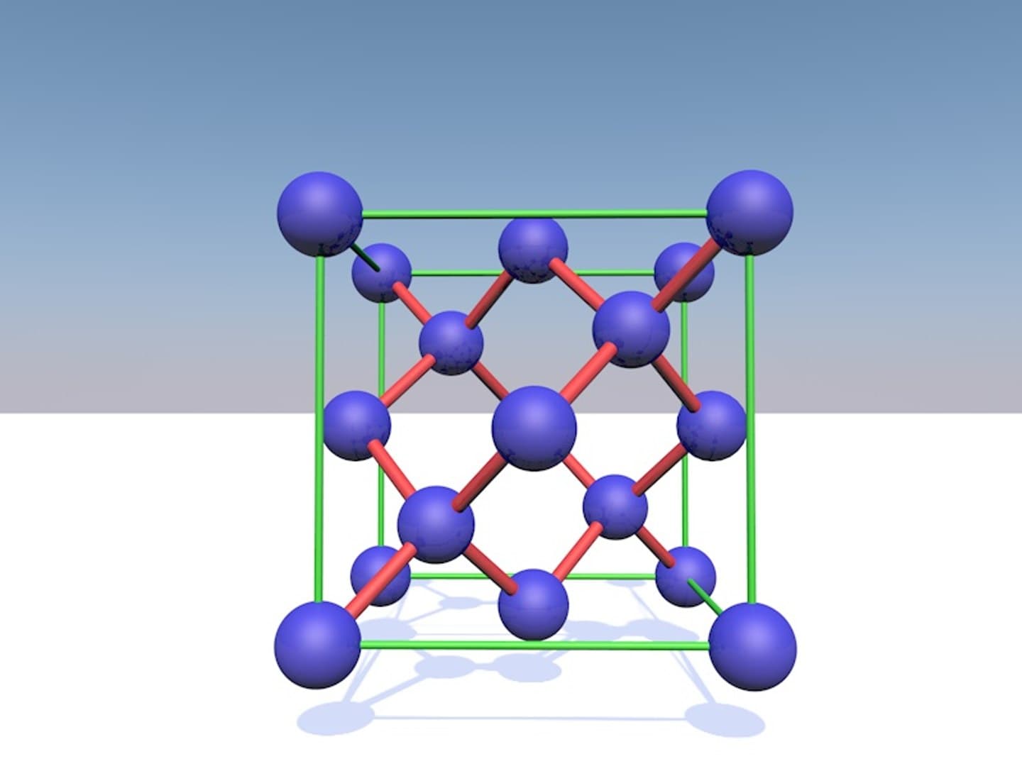
A silicon atom has four outer valence electrons. These are electrons it wants to share. In a pure crystal, every silicon atom bonds to four neighbors, and those neighbors bond to four more, repeating in a perfectly regular three-dimensional grid called a lattice. Because all the electrons are tied up in bonds, perfectly pure silicon barely conducts electricity at all, which makes it useful, because we can then control its conductivity precisely.
How the crystal is made
Silicon crystals do not grow in perfect form naturally. Ultra-pure silicon is melted in a crucible, and a small "seed" crystal with the exact atomic arrangement we want is dipped into the molten surface. The seed is then slowly pulled upward while rotating, and atoms from the melt latch onto it and snap into alignment with the seed's lattice. The result is a single flawless cylinder of crystal (a "boule") that can be over a meter long, which is then sliced into the thin round wafers chips are built on.
Doping with boron and phosphorus to make + and -
Pure silicon barely conducts, as every electron is locked into a bond. To make it useful, we deliberately contaminate it with tiny amounts of other atoms through doping.
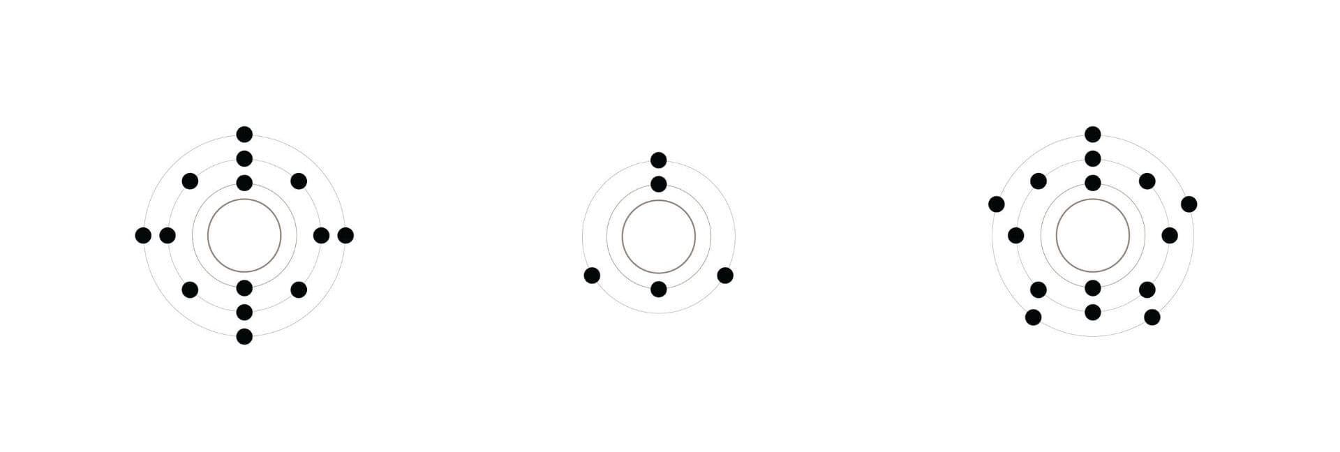
Phosphorus has five outer electrons. Drop a phosphorus atom into the lattice and it bonds with four silicon neighbors, leaving one electron with nothing to do. This spare, loosely held carrier is free to roam and conduct. Silicon doped this way has extra negative carriers, so we call it n-type. Boron has only three outer electrons. It bonds with its neighbors but leaves one bond unfinished. This vacancy, or hole, behaves like a mobile positive charge. Silicon doped with boron is p-type.
Using a patterned mask, we expose only selected regions of the wafer, then fire boron or phosphorus atoms into those spots. By choosing which patches become n-type and which stay p-type, we draw the sources, drains, and channels of millions of transistors directly into the crystal. Doping is what turns a uniform slab of silicon into an actual circuit.
Phonons
The atoms in the lattice jiggle, and those vibrations come in discrete packets of energy called phonons, the vibrational cousin of how light comes in packets called photons. Phonons are how heat moves through the crystal, and they constantly bump into electrons, knocking them off course. They matter for our story because heat is the enemy of a chip that has to sit inside a living body, and the same jostling that carries that heat also nudges the electrons we are trying to control.
Electrons and bands
In a single atom, electrons sit at fixed energy levels, but in a crystal of billions of atoms those levels smear into broad bands of allowed energy. Two bands matter. The valence band is where electrons are locked into bonds, and the conduction band is where they're free to roam and carry current. Between them sits a forbidden gap (~1.1 electron-volts in silicon). Give an electron enough energy from heat, light, or an electric field, and it jumps the gap into the conduction band, leaving behind a positively charged empty spot called a hole. By deliberately adding trace impurities ("doping"), we can stock the silicon with extra free electrons or extra holes, tuning exactly how and where it conducts.
Gates
A gate is a small conductor laid just above the silicon but separated from it by an ultra-thin insulating layer (typically an oxide). Put a voltage on the gate and its electric field reaches through the insulator into the silicon below, pulling carriers in or pushing them away, which opens or closes a conducting channel without ever physically touching it. That's the entire trick of a field-effect transistor. A gate voltage acts like a valve on a stream of electrons.
MOSFET
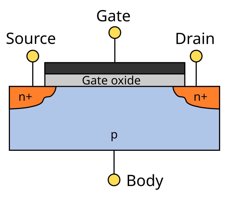
Ok. We have the pieces. Stack the pieces and you get the MOSFET, the workhorse of every chip. Take a slab of p-type silicon and embed two n-type regions a short gap apart. One is the source, the other the drain. Lay an ultra-thin insulating layer of oxide over the gap, and put a gate on top of the oxide. The gate hovers just above the silicon, separated from it only by that sliver of insulator.
The device is simply a voltage-controlled switch. With the right voltage on the gate, its field reaches through the oxide and pulls a conducting channel into existence beneath it, and current flows from source to drain. Remove the voltage and the channel vanishes, cutting the current off. A small voltage on the gate governs a much larger current underneath it, and it does so while drawing almost no current itself, because the oxide is an insulator. Almost. That leak is where we are headed. The gate and the silicon never touch.
Why you need large resistors in an ASIC
The simplest filter is built from a resistor and a capacitor working together.
The capacitor blocks slow voltages and passes fast ones, while the resistor treats every frequency the same.
So in a chain the two form a divider whose cutoff lands where the capacitor's frequency-dependent resistance equals the resistor's. The larger the resistance, the lower that cutoff, and to block the slow electrode drift while preserving a neural signal, it has to sit below about a single hertz.
Capacitors take up precious die area, so they're kept small, which forces the resistance to be enormous, on the order of billions to trillions of ohms, just to reach such a low cutoff. Multiply that by thousands of recording channels on one chip, and an ordinary resistor (whose size grows with its resistance) becomes unfeasible, particularly for something implanted inside a human being. You need a way to make a gigantic resistance in almost no space.
Quantum tunneling
An electron is a spread-out wave of probability, and that wave leaks into the oxide and fades. If the oxide is thick, the wave fades to almost nothing before reaching the far side, and in practice the electron never crosses. But if the oxide is just a few atoms thick, a sliver of that wave survives to the other side, which means there is a small but real chance the electron simply appears across the wall. That is quantum tunneling. The electron's probability of crossing the barrier is bleeding through.
The current that tunnels across is tiny. A tiny current under a given voltage is the definition of an enormous resistance! So we turn the flaw into the device. Tie the source and drain together so the transistor isn't switching anything, and treat the path through the oxide as the component itself.
What we've built is a resistor of billions to trillions of ohms (gigaohms to teraohms) living in the footprint of a single transistor. And because tunneling responds so steeply to voltage, the resistance is tunable. Shift the gate's operating point and it moves; wire a few in parallel to step the resistance down, then trim the bias, and you can place the filter's cutoff where you want it.
That is the magic of quantum tunneling in field effect transistors. Thousands of these resistors fit on a die small enough to live inside the body, each one holding back electrode drift so that the faint voice of a single neuron can be heard.